Creating a Custom PCB With KiCad 7
Are you interested in creating PCBs? KiCad offers a simple and free way to design your own PCBs and have them manufactured. Let’s take a look!
Introduction
Makers often find that prototyping electronics projects can get quite complex over time, and the use of breadboards and jumper wires can become difficult to manage.
PCB design offers a way to create a custom board that can be used to clean up the prototyping process, and can also be used to create a final design. Especially now with companies like JLCPCB offering PCB manufacturing for as little as $2, it is often easier to create a PCB for projects you’d like to keep or share with others than other alternatives.
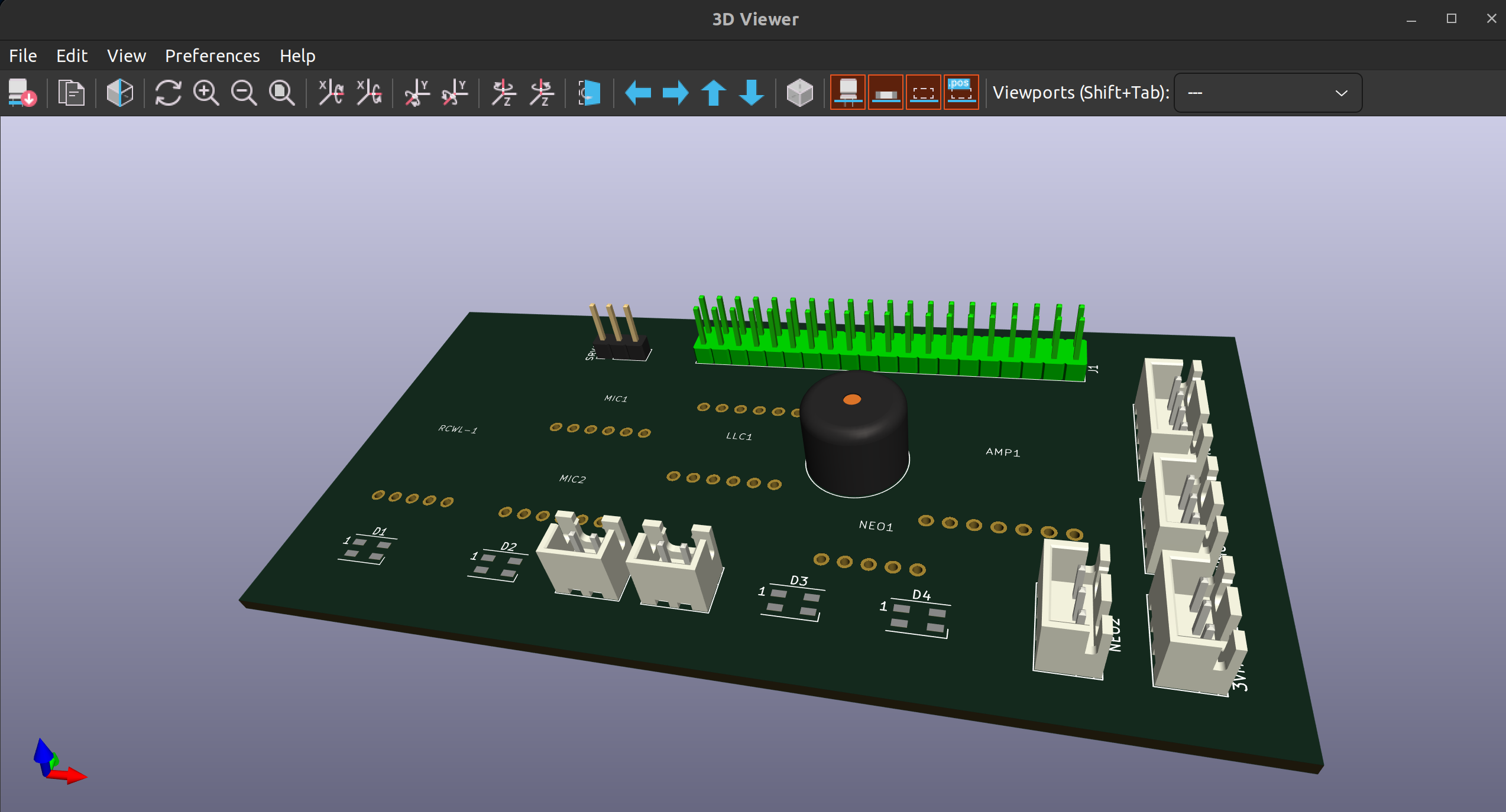
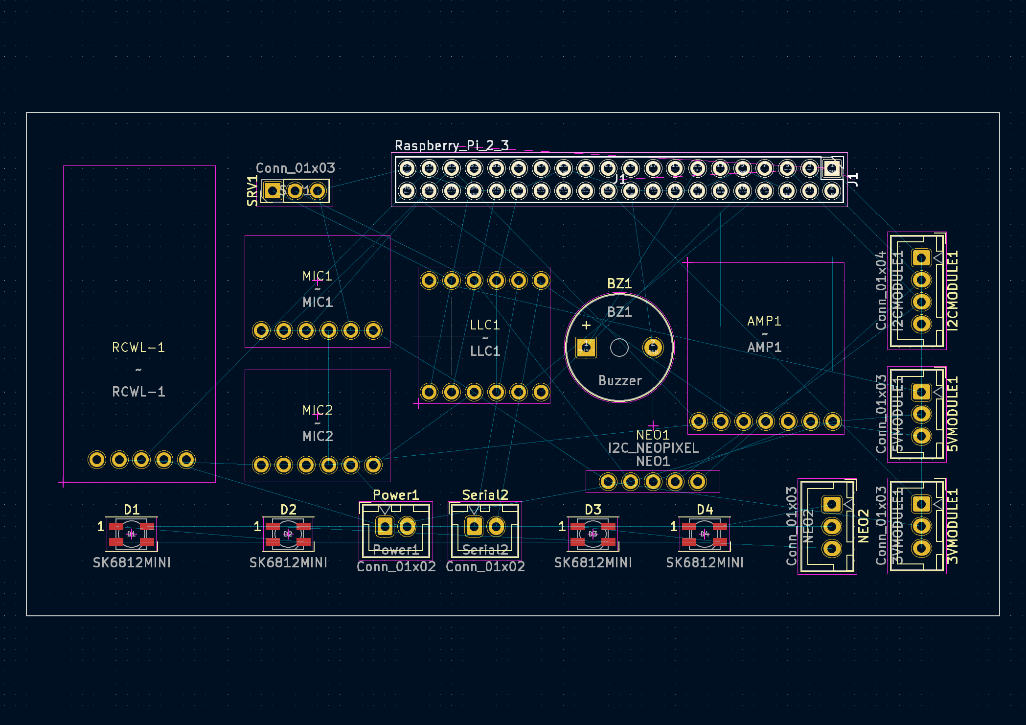
I have created a few PCBs over the time I have been working on the modular biped, and with the release of the new Raspberry Pi 5, I wanted to take the opportunity to clean up the design by creating a new PCB for the project.
I wanted to be able to create a PCB with multiple layers and allow the third party modules that it uses to be connected to the new Raspberry Pi 5. I had difficulty finding these modules available in my current PCB design software, so I wanted to try a tool that allowed me to create my own parts library easily.
For these reasons I decided to take a look at using KiCad. Let’s take a look at the process below.
Installation
You can install KiCad on Windows, Mac, or Linux. I am using Ubuntu 20.04, and the installation instructions can be found here:
1
2
3
sudo add-apt-repository ppa:kicad/kicad-7.0-releases
sudo apt update
sudo apt install kicad
Getting started
When you open the main KiCad application you will see the following screen, which contains links to the various tools.
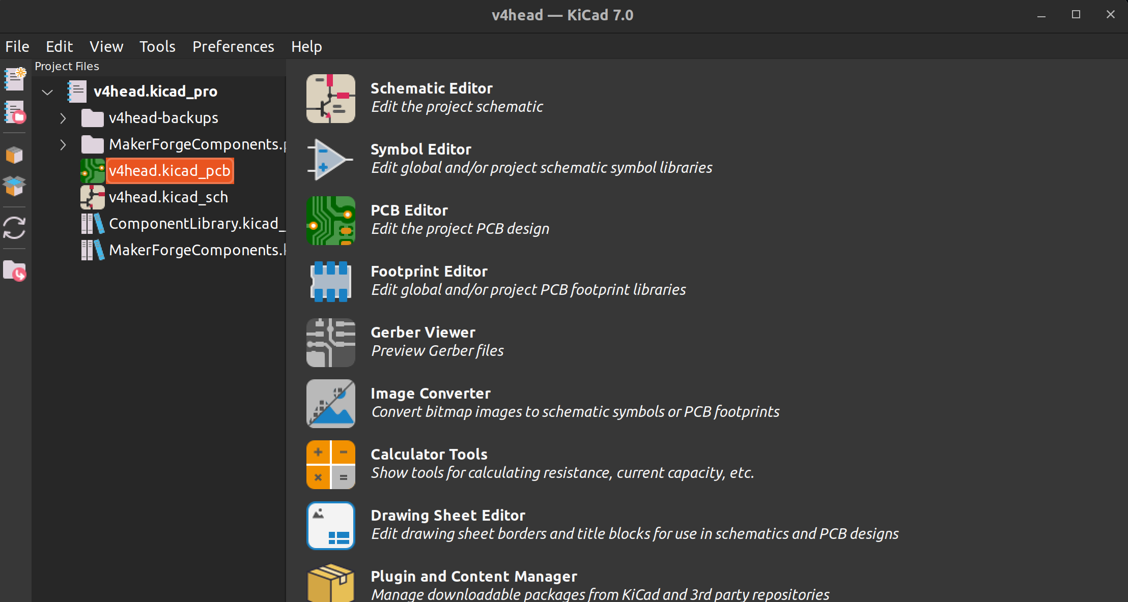
The tools I will be discussing are the Schematic Editor, the Symbol Editor, the Footprint Editor and the PCB Editor. Let’s take a look at each of these in turn.
Schematic Editor
This is the tool that allows you to create the schematic for your PCB. You can add components from the library, and connect them together using wires. It is also possible to add text and other annotations to the schematic.
You also link a footprint to a symbol here, which is the physical layout of the component on the PCB (see below).
Symbol Editor
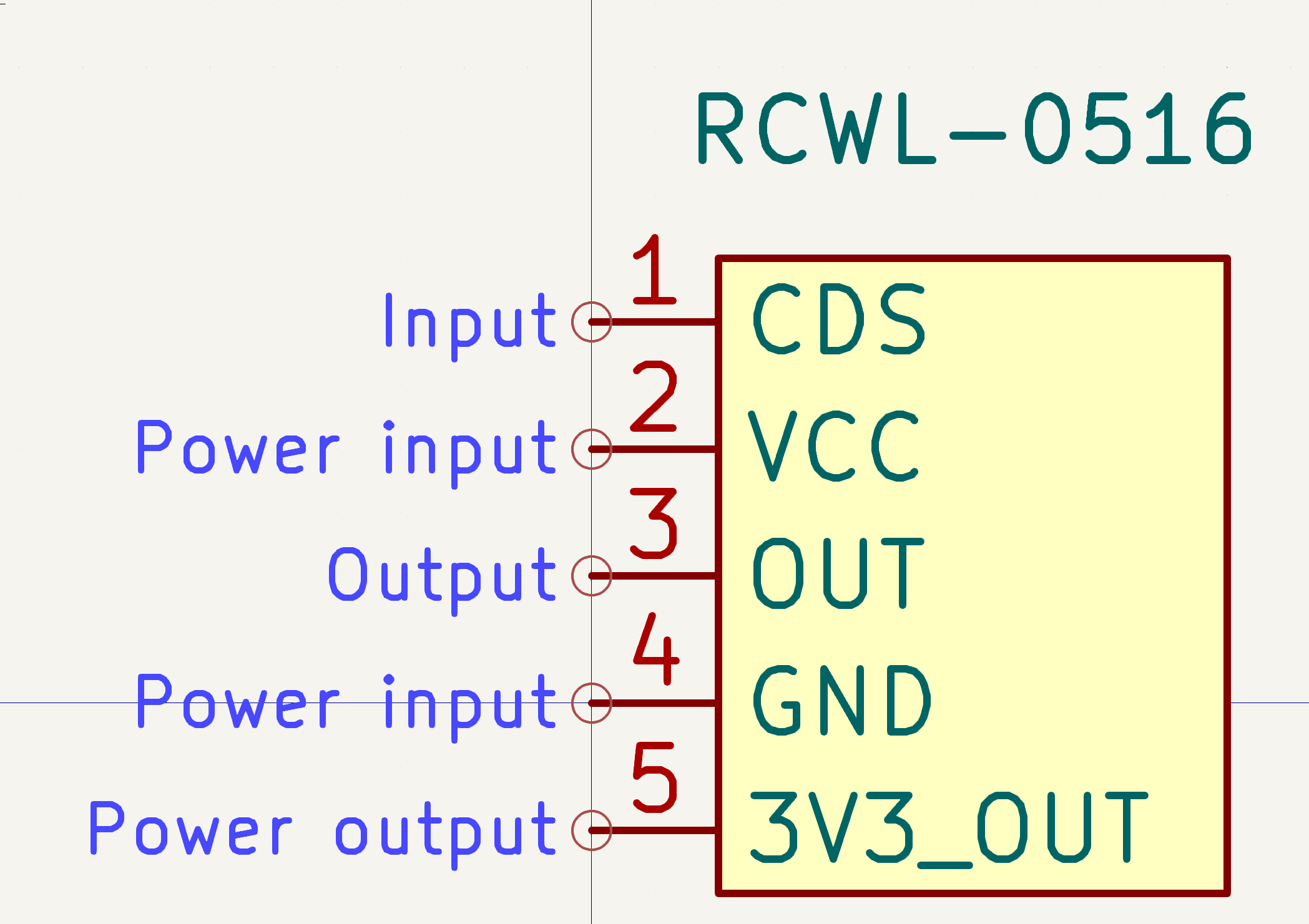
This tool allows components and component libraries to be created, for use in the schematic editor. To create a new component you can define the pins and layout of the component, and then add this to a library.
Footprint Editor
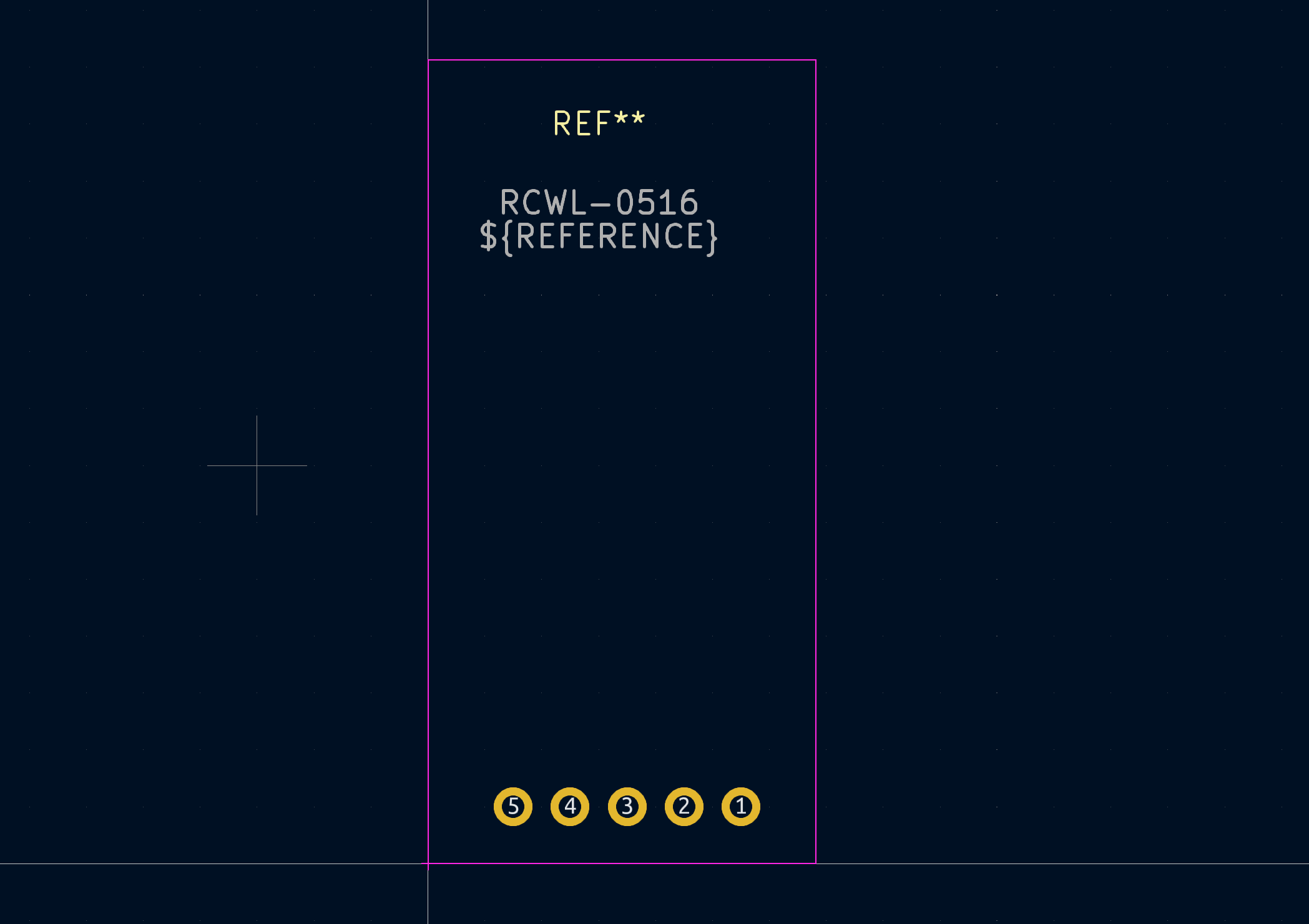
Separate to the symbol, the footprint is the physical layout of the component on the PCB. This tool allows you to create the footprint for a component, and add it to a library.
PCB Editor
This tool allows you to create the PCB layout, and add the components and footprints to the PCB. You can also define the layers of the PCB, and the rules for the PCB design.
Creating a new project
To create a new project, click on the “Create a new project” link on the main screen. This will open a new window, where you can select the project name and location.
Create a new symbol
You can create a new symbol and library in the Symbol Editor.
File -> New Library...
The library acts as a central location for your symbols. Once you have this in place, create a new symbol by clicking on the “Create a new symbol” button or press N.
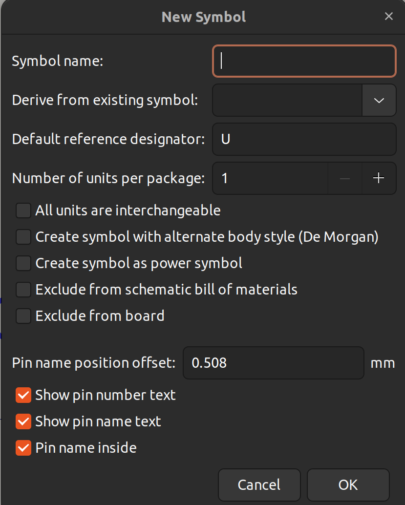
Once created, you can define the number of pins, the type and location, as well as the name. Click on the Add a pin button to add a new pin or type P.
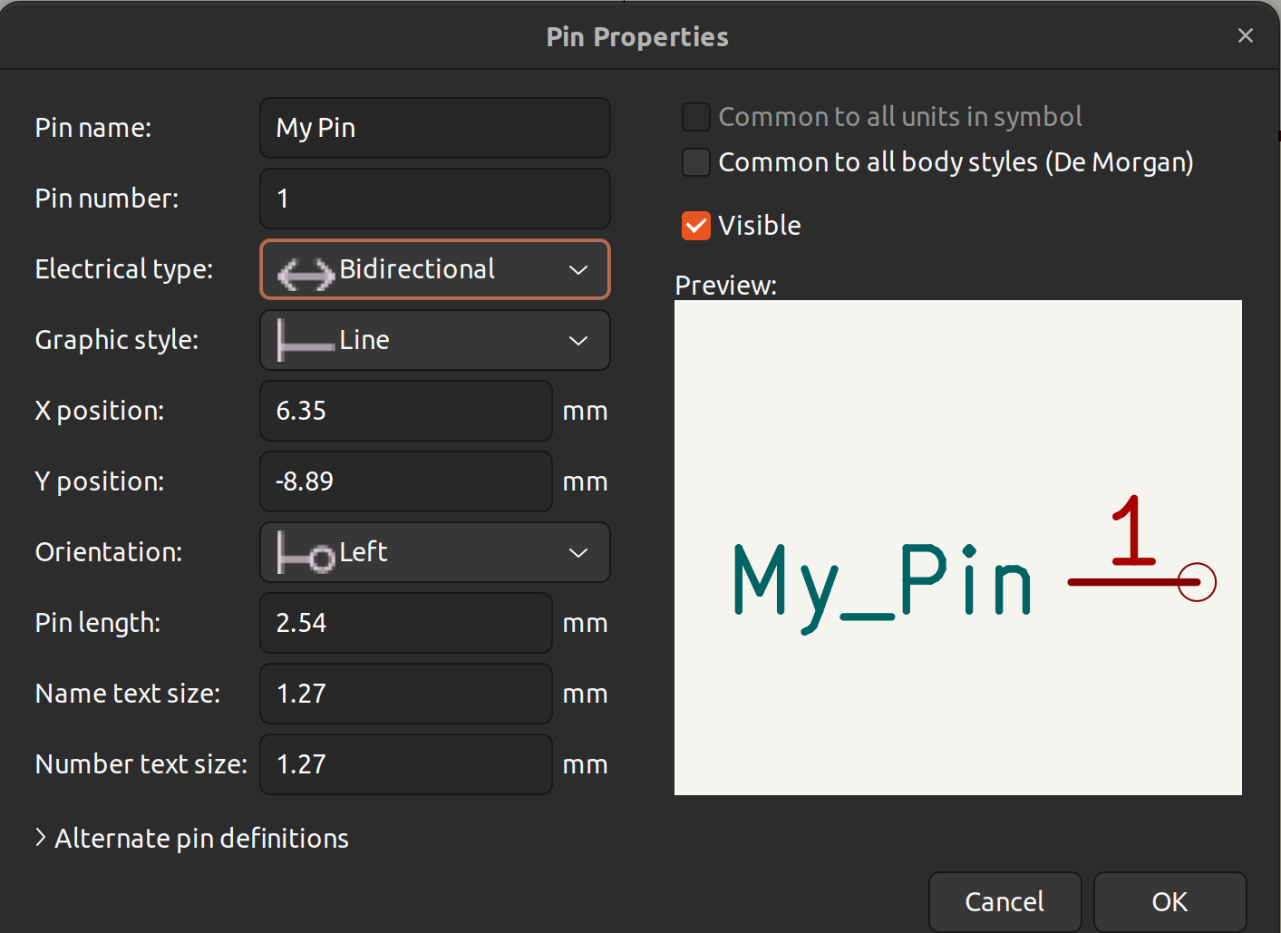
You can then position the new pins and add a rectangle to represent the component. Double clicking on the rectangle allows you to fill the body with a colour.
Once you have completed the symbol, save and navigate to the footprint editor.
Create a new footprint
Each symbol should have a matching footprint, these are linked in the schematic editor but defined in the footprint editor.
In the footprint editor, you can define a new custom library.
File -> New Library...
Once the library is defined you can create a new footprint with the New Footprint button or by pressing Ctrl+N and entering a name.
The footprint editor allows you to place pads for each pin defined in the symbol, so make sure you are using the positioning them correctly. You can use the grid to help you align the pads.
Typically, headers (such as the 40 pin header on the Raspberry Pi) have a 0.1” pitch (or 2.54mm), you can select this grid from the top menu.
Once the pads have been positioned you can switch to the layer F.Courtyard and draw a rectangle around the pads. This will be used to define the outline of the component on the PCB.
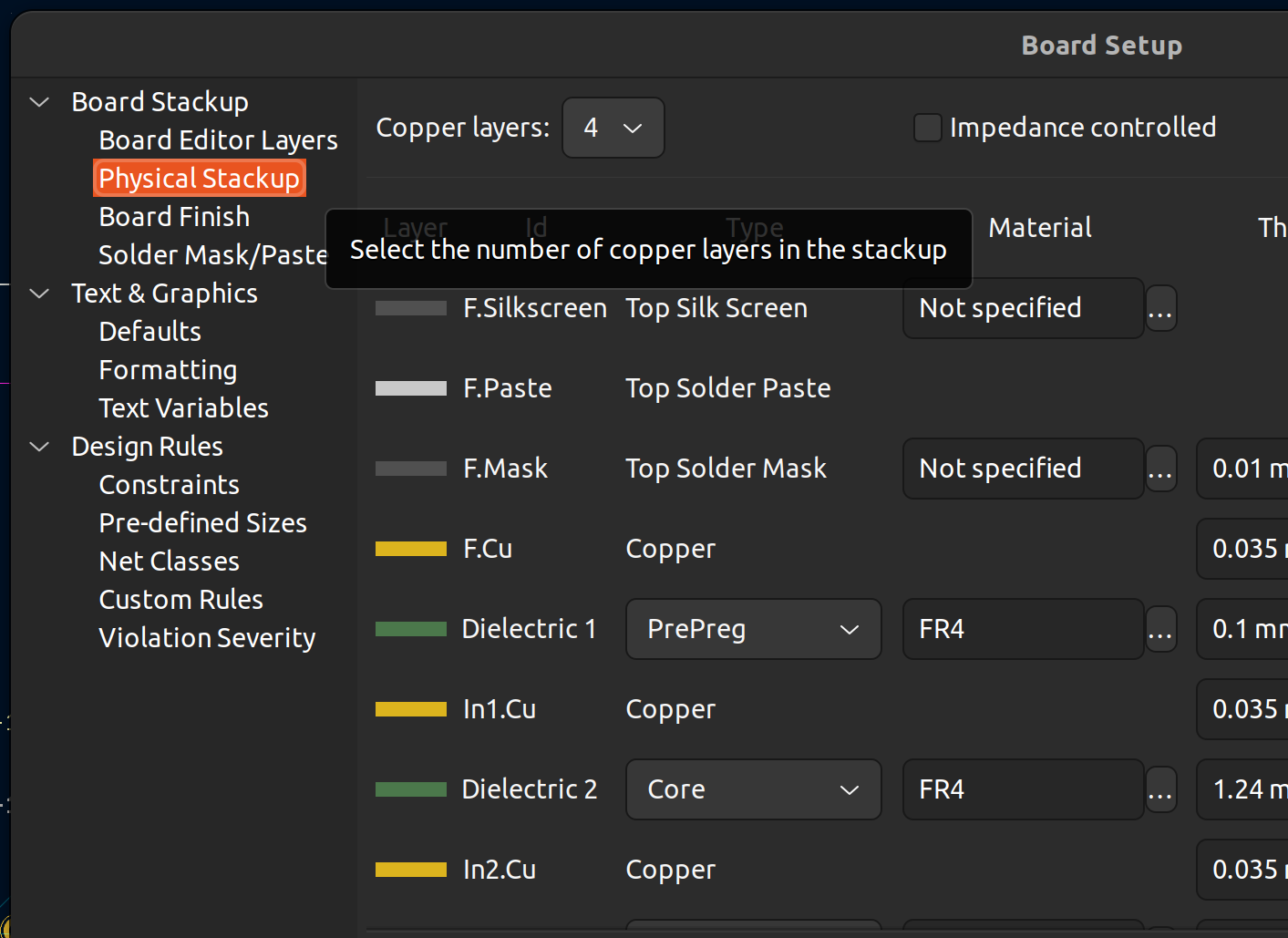
A note on layers
Layers are used to define where an element in the editor features (on or off board, which side of the board, etc). Simple PCBs are typically two layers, but more complex PCBs can have up to 16 layers. There are also layers defined for the silkscreen, solder mask, and other elements of the PCB.
To create a PCB with more than two layers, go to File -> Board Setup in the PCB editor and select the number of copper layers you want to use.
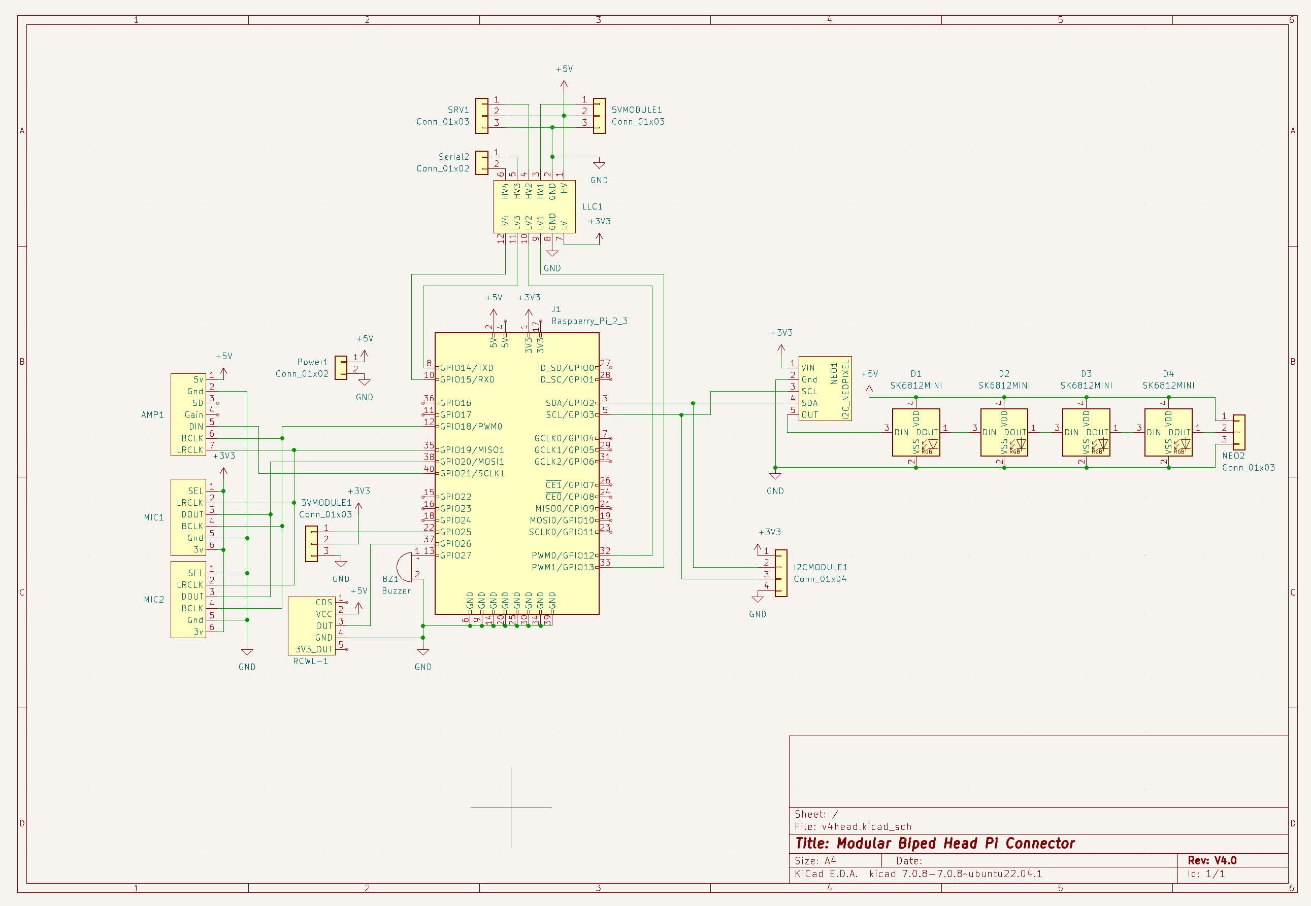
Design your schematic
Once you have created your symbols and footprints, you can start to design your schematic. Open the schematic editor and create a new schematic.
Drop your components onto the schematic and connect them together using wires. You can also add text and other annotations to the schematic.
Once you have completed the schematic, you can move to the PCB editor and position the components.
Use the command Tools -> Update PCB from Schematic to update the PCB with the components from the schematic.
Footprints can be rotated and positioned to allow for easy routing of the PCB.
Routing the PCB
Routing is the process of connecting the components on the PCB. This can be done manually or automatically, although manually is generally preferred as it allows for more control over the routing.
You should see faint lines between the pads on your footprints that represent the connections made in the schematic editor. Routing allows you to connect these pads together on the PCB with ‘traces’ (also called ‘tracks’), and specify the thickness and spacing. Remember that some traces will need to be thicker than others to carry more current.
Autorouting is also an option with plugins.
Power planes
Power planes are used to provide a large area of copper for power and ground connections. These are typically used for high current connections, such as the power supply.
In the PCB shown, I am using a 4 layer PCB with power planes (5v and ground) on the two middle layers. This allows me to connect the power supply to the power planes, and then connect the components to the power planes rather than connecting traces which would be very complex and difficult to route.
Exporting for manufacturing
Once you have completed the PCB design, you can export the design for manufacturing. This will create a set of files that can be sent to a PCB manufacturer.
File -> Fabrication Outputs -> Gerber
File -> Fabrication Outputs -> Drill Files
This will create the necessary files for the PCB manufacturer. You can then zip them and upload to the manufacturer of your choice.
I recommend JLCPCB, as they offer a very good service and are very affordable. You can find out more about their service here.
Video Overview
To see how this works in practice, take a look at the build log below on YouTube:
References
https://learn.sparkfun.com/tutorials/beginners-guide-to-kicad/all